


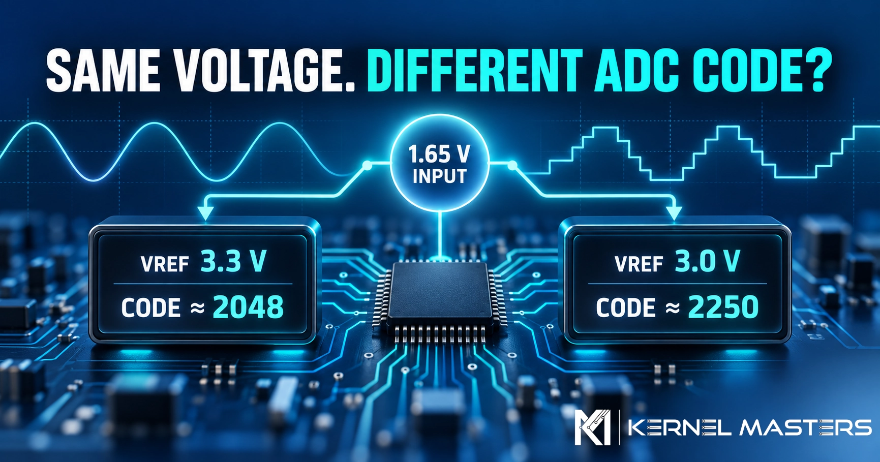
2047, 2048, 2047, 2048 looks like a reassuringly stable ADC reading. But what if the voltage calculated from those codes disagrees with the voltage at the MCU input pin?
The ADC register contains a digital code, not a measurement already expressed in volts. That code depends on the voltage captured during sampling and the reference used during conversion. A repeatable code can therefore be a repeatable error.
We will use the 12-bit SAR ADC in the Raayan Mini’s STM32F401RB to follow the signal through the circuit. Other ADC architectures can acquire signals differently; the switched-capacitor timing details below describe this STM32 example.
1. The code is a ratio
The STM32 ADC compares its captured input with its reference. A 12-bit result has 4096 possible codes: 0 to 4095. One ideal LSB spans VREF / 4096 volts. For a quick estimate away from the range limits:
ADC code ≈ (captured input voltage / VREF) × 4096, limited to 0–4095.
Real codes are quantized and affected by the ADC’s own errors, so the following numbers are illustrative estimates, not guaranteed readings.
With a fixed 1.65 V at the input and VREF at 3.3 V, expect a code near 2048. Keep the input at 1.65 V but lower VREF to 3.0 V, and the expected code moves to roughly 2250. The input stayed fixed; its ratio to the reference changed.
Fixed input · VREF 3.3 V
Code ≈ 2048
1.65 ÷ 3.3 = 0.50 of full scale
Same input · VREF 3.0 V
Code ≈ 2250
1.65 ÷ 3.0 = 0.55 of full scale
A useful exception: if the input itself follows the same supply as the reference, both can move together and the code may remain nearly unchanged. A divider or potentiometer powered from the ADC reference can behave this way. Verify the actual board connections before treating a particular sensor as ratiometric.
On the STM32F401RB, VREF+ is internally tied to VDDA and VREF− to VSSA. A firmware constant of 3.3 V does not force the board’s analog supply to be exactly 3.300 V.
2. What reaches the sampling capacitor?
The F401’s SAR ADC has a switched-capacitor input stage. During the programmed sampling time, an internal switch connects the selected channel to a sampling capacitor. During the conversion phase, the captured charge is used by the SAR circuitry to produce the code.
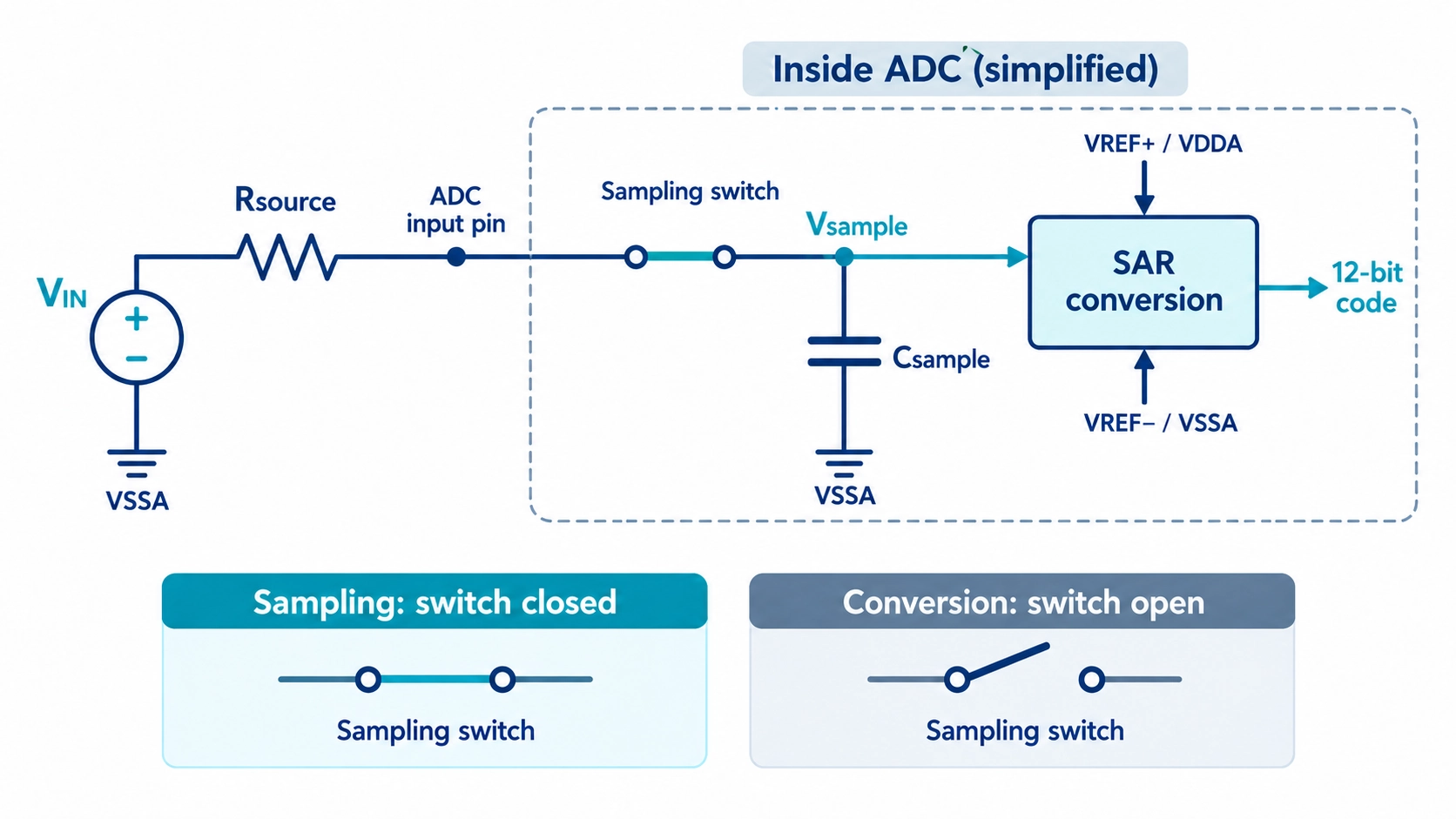
Functional model of the sampling path. The capacitor and switch explain acquisition; the reference participates in conversion. This is not the physical silicon schematic.
The diagram is a functional model, not a transistor-level drawing of the silicon. Rsource includes the resistance of the sensor, divider, or conditioning circuit. The ADC switch has its own resistance; the pin and PCB also add capacitance. These details matter when selecting a sampling time.
If the switch is open before the capacitor has settled near the new input, conversion uses the capacitor voltage that was reached—not necessarily the voltage currently present at the sensor output. For a simplified RC model:
Vsample(t) = VIN + (Vinitial − VIN) × e^(−t/τ), where τ ≈ (Rsource + Rswitch) × Csample.
This explains the direction of the error; it is not a substitute for the device’s input-impedance and sampling-time specifications. ST provides those conditions in the datasheet and AN2834.
For 12-bit operation, the F401 reference manual gives a total conversion time of sampling time + 12 ADC clock cycles. Sampling-time settings range from 3 to 480 cycles, chosen per channel. More time can improve settling for a difficult source, but it also reduces the attainable conversion rate.
3. Why channel order can matter
Imagine a scan reading a channel near 3.0 V, then one near 0.5 V. Charge remaining in the input network can make the second channel’s early sample too high if it cannot settle in time. Internal switching also affects the starting charge; the simple RC picture is only a teaching approximation.
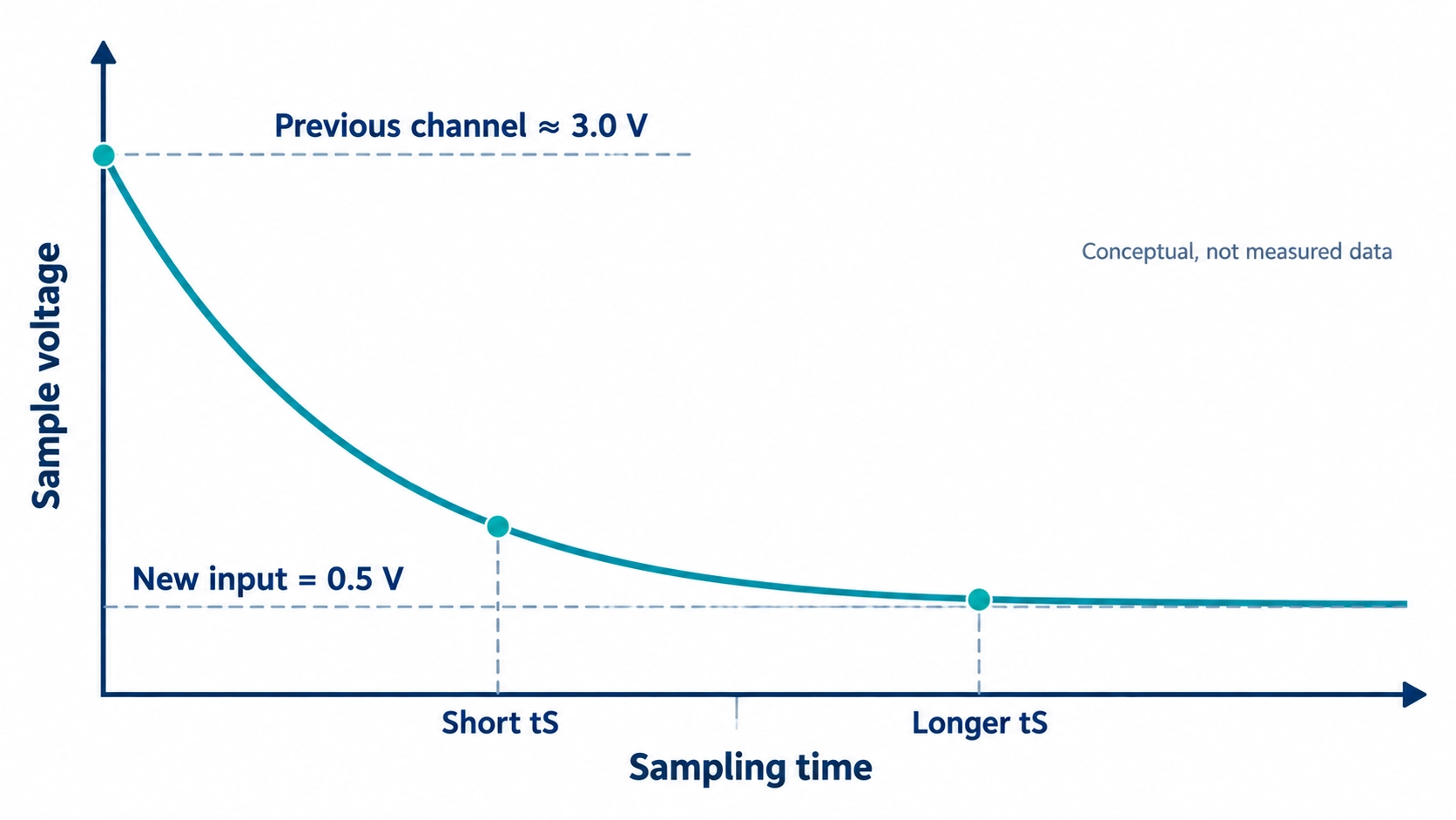
Conceptual response after switching from a high channel to a lower channel. A longer acquisition interval can reduce the settling difference; this is not measured Raayan Mini data.
This is a possible mechanism, not a prediction that the first conversion is always wrong. A practical test is to compare the suspect channel alone and within the scan, then change its sampling time and channel order. If the reading moves, investigate impedance and settling before changing the voltage formula.
4. A stable code does not prove accuracy
Noise and resolution are only part of measurement quality. The input might be steady at the sensor and different at the MCU pin. VDDA may differ from the number used in firmware. Ground voltage can move under switching currents. Filtering can make an offset reading look even steadier.
| Term | What it tells you |
|---|---|
| Resolution | How finely the input range is divided into codes. |
| Repeatability | Whether repeated readings are similar. |
| Accuracy | Whether the result is close to the quantity being measured under known conditions. |
A 12-bit converter offers fine code steps. It does not promise 12-bit system accuracy. Compare a measurement against a suitable known input or instrument, and include the sensor and analog circuit in that comparison.
5. Debug the complete measurement path
- Capture raw codes. Temporarily remove display scaling and filtering from the investigation.
- Measure at the MCU input. Check against the sensor output; a discrepancy between the two points indicates something in the board signal path.
- Check the analog reference path. On the F401RB, determine VDDA rather than assuming the firmware’s
3.3 Vconstant is the measured reference. - Lengthen the channel’s sampling time as a test. Improvement is evidence to investigate settling and source impedance; it is not a complete diagnosis on its own.
- Read one channel, then scan several. Compare channel order to reveal possible charge or timing interactions.
- Check time-varying signals with a scope. A meter’s averaged voltage and an ADC’s instantaneous samples may legitimately differ. Observe the same point and timing.
- Recheck the calculation. Apply the actual reference, ADC code range, and sensor transfer function only after understanding the raw measurement.
Bringing the idea to Raayan Mini
Raayan Mini training uses an analog potentiometer and an LM35 temperature sensor. The LM35’s nominal output scale is 10 mV/°C; its output and supply must not automatically be treated as the ADC’s reference. A potentiometer is useful for moving an ADC input across its range, but whether it is ratiometric depends on how its ends are powered on the board.
The next step for a board-specific lab would be to record the board revision, exact input channel, analog supply, sampling-time setting, voltage at the MCU pin, and raw code. Until then, the diagrams and numbers here explain principles rather than claim a measured result from this board.
Takeaway
The code represents what the sampling network captured relative to the reference. When the value seems wrong, trace the signal from the source through the input network, reference, and conversion settings before trusting the displayed number.
 Admission for 6 months Embedded AI & IoT offline course at Hyderabad & Bangalore
 Course Fee: ₹12000 /-